
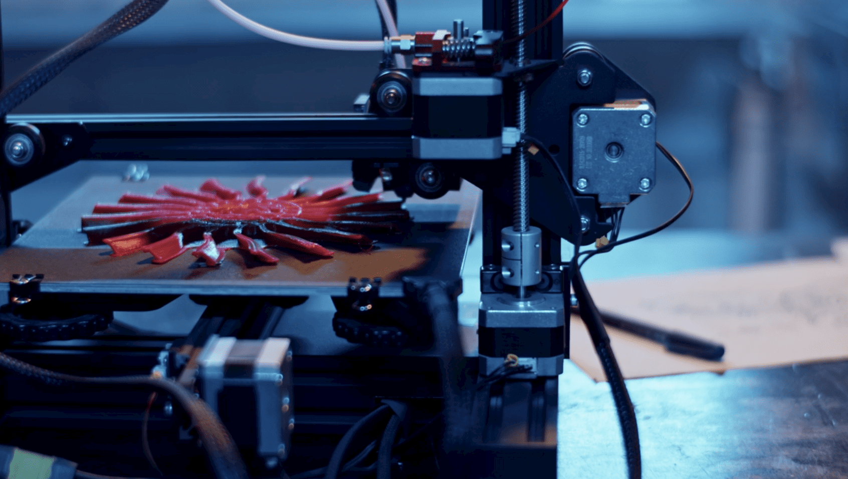
3D printing technology is already very mature. As early as 2021, 3D printing robots can print a 1,900-square-foot detached house out of concrete in 48 hours, including three bedrooms and two bathrooms with bathtubs. And the cost is only half of traditional house building methods.


What Are the Difficulties in Making Chips
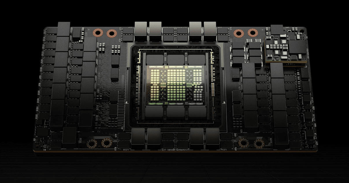
We all know that manufacturing chips is incredibly difficult. Nvidia founder Jensen Huang pointed out that advanced chip manufacturing requires more than 1,000 steps to produce features the size of a biological molecule. Every step must be nearly perfect to produce a functional output. Nvidia’s H100 GPU, a chip designed for generative AI, sells for an average of $30,000 per chip, which is one of the reasons for its stellar performance.
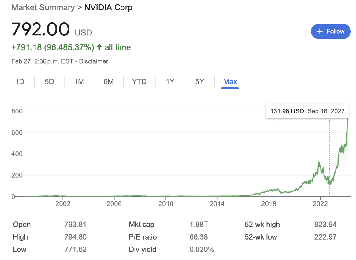
According to its fiscal year calculation, as of the fourth quarter financial report on January 28, 2024, revenue for the quarter was US$22.1 billion, an increase of 22% from the previous quarter, and an increase of 265% from the same period last year. Nvidia’s stock price soared to $792 per share.
If 3D printing technology can be directly applied in chip manufacturing, it will bring huge advantages. First, 3D printing does not need to open molds, eliminating expensive upfront costs, and allows for flexible processing and printing according to the structure of each chip. Secondly, 3D printing technology can reduce the number of steps in the chip processing process, including lithography, etching, polishing, deposition etc., thus saving a lot of equipment costs, as well as compatibility and cooperation issues between various equipment.
Since 3D printed chips can bring many benefits, why is there no mature technology yet? Because 3D printing technology has a weakness, that is, the accuracy of printing is not high enough. 3D printing generally needs to heat the materials until it melts, then spraying the melted material to the target location, and waiting until the material cools down to re-solidify to the desired shape. During the period of cooling and solidification, the melted material can flow, and some materials flow to other places before they have time to be fixed, deviating from the targeted position. This makes accuracy not high enough. Don’t worry, this problem has been solved.
How to Solve the Problem of Low Precision of 3D Printing Technology
The accuracy of 3D printing is generally 1/10 mm, while the chips produced by the wafer factory are nanometer-level accurate. How to solve the accuracy problem of 3D printing technology?
Note: A human hair is divided into 100,000 equal parts, and each tiny segment is about one nanometer thick.
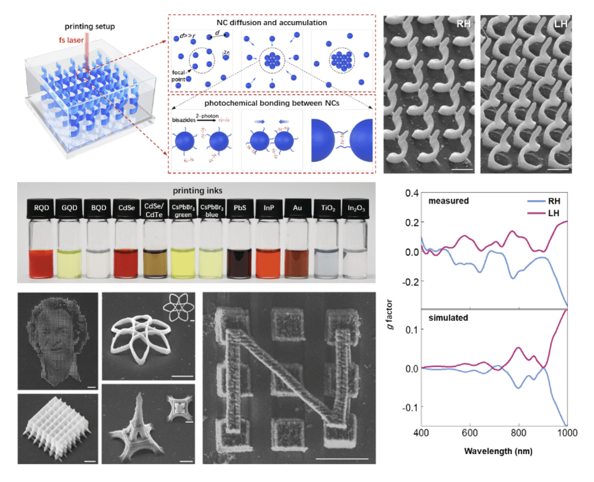
In December 2022, Leon Zhao of Carnegie Mellon University and Shih-Chi Chen of the Chinese University of Hong Kong published a paper in Science magazine in which they developed a strategy for creating ultra-high-resolution 3D nanostructures utilizing a variety of materials to reduce the size of printable nanodevices to a dozen nanometers or a few atoms thick. Their solution was to create a three-dimensional pattern of the materials in a hydrogel and then shrink them to obtain nanometer-scale resolution.
What’s New in 3D Printed Chips
The difficulty of 3D printing chips, if you look at their chemical nature, is that the stability of the 3D printed structure comes from the chemical bonds between atoms or molecules in the printed material. Inorganic materials such as semiconductors or metal oxides are difficult to form bonds under 3D printing conditions, and so polymers are often needed as templates. The mixture printed in this way has low purity and cannot maintain the original material properties.
What to do? The team of Academician Li Jinghong from the Department of Chemistry of Tsinghua University and the team of Professor Sun Hongbo from the Department of Precision Instrumentation have developed a new method for nanometer-level precision 3D printing of inorganic materials without polymer templates (referred to as 3D Pin). For the first time, they used nanometer crystalline materials enable nanoscale precision 3D printing.
On September 29, 2023, they published their research results in Science under the title “3D printing of inorganic nanomaterials by photochemically bonding colloidal nanocrystals”.
Simply put, this method eliminates hybrid approaches. First, the 3D printing material is made into a nanocolloid. The colloid itself forms a protective layer over the printing materials. The colloid is then modified with a substance called nitrene, so that the material will not be uneven. Here is Tsinghua University’s explanation of the study:
“ 3D Pin method uses colloidal nanocrystalline solutions as the raw material “ink” of the corresponding inorganic materials, and designs a small molecule cross-linking agent based on photogenerated nitrene radicals, which utilizes femtosecond lasers to trigger photocross-linking reactions of ligands on the surface of the nanocrystals so that stable covalent bond connections are formed between the nanocrystals, thus realizing the universality and high purity of the materials (mass fraction >90% of the inorganic component). The 3D printing of inorganic materials with universal applicability, high purity (mass fraction of inorganic components is more than 90%), and high precision (breaking through the limit of optical diffraction, with a resolution of up to 150 nanometers) has been realized.”
Of course, this research is still a long way from 3D printed chips. The method of modifying the nanocolloids uses the substance nitrene. This synthetic method is difficult to mass-produce and needs further optimization. In addition, what kind of 3D printer can match such a printing process, and whether it can be commercialized still needs time to test.